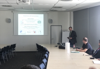
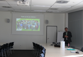
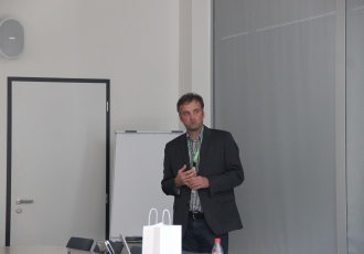
- Speaker: Prof. Oliver SCHMIDT
- Institution: Institute for Integrative Nanosciences, Leibniz IFW Dresden, Germany
- Invited by: Mgr. Vlastimil Křápek, Ph.D.
- Date: 30.10. 2018
- Place: CEITEC Brno University of Technology
Anotation:
Nanomembranes are thin, flexible, and transferable and can be assembled into 3D micro and nanoarchitectures. In case optically active nanomembrane materials are selected many new research paths and exciting future application scenarios open up in nanophotonics. For instance, we have exploited semiconductor nanomembrane materials including high quality quantum emitters to create highest speed [1], highest yield [2], highest brightness [3] and Si-integratable [4] sources of entangled photons, which could lie at the heart of future quantum communication technologies.
If nanomembranes are differentially strained they deform themselves and roll-up into microtubular structures upon release from their mother substrate. Photonic rolled-up microtubes can be exploited as 3D microcavities to study spin orbit coupling of light [5] or selective opto-plasmonic coupling in vertical ring resonators [6]. Fully on-chip integrated systems offer interesting options for 3D photonic integration and lab-in-a-tube concepts.
[1] J. Zhang, J. S. Wildmann, F. Ding, R. Trotta, Y. Huo, E. Zallo, D. Huber, A. Rastelli, O. G. Schmidt, Nature Commun. 6, 10067 (2015)
Photogallery


 Share
Share


